Where neural networks are being deployed in semiconductor manufacturing and how well they’re performing.
Copyright: semiengineering.com – “Improving Yield With Machine Learning”
Image source: Synopsys/IEEE ASMC
 Machine learning is becoming increasingly valuable in semiconductor manufacturing, where it is being used to improve yield and throughput.
This is especially important in process control, where data sets are noisy. Neural networks can identify patterns that exceed human capability, or perform classification faster. Consequently, they are being deployed across a variety of manufacturing processes to spot defects and determine whether they will affect the functioning of a device over its anticipated lifetime.
“A lot of AI stuff is starting to happen now, where customers are identifying the most relevant measurements,” said Subodh Kulkarni, president and CEO of CyberOptics. “We extract the outliers, and the integration happens one level above, leading to new levels of yield improvement.”
Machine learning has been in use in the inspection arena for the longest of any manufacturing process, and it is being incorporated into new tools. Algorithms can isolate defect signatures or patterns that are unknown to the yield engineer.
“KLA’s broadband optical inspection systems have on-tool binning technology that uses defect attributes to separate detected events into different defect types and nuisance defects using machine learning,” said Satya Kurada, vice president of marketing at KLA.
Thank you for reading this post, don't forget to subscribe to our AI NAVIGATOR!
Defects identified on optical tools that require additional classification are typically reviewed on e-beam inspection systems. “Fab engineers use the defect information to optimize the production line,” Kurada said. “The end result should be more good die making it to end of line, where probe takes place.”
Like the human brain, deep learning (DL) recognizes patterns and uses that information to judge incoming data automatically. Using a cascade of multilayer, nonlinear processing units for feature extraction and transformation, each layer in a neural network uses the output of the previous layer as input for the next layer. In defect inspection, DL- or ML-based algorithms reduce the burden of manual classification and reduce time to result.
The automated nature of the networks also makes them attractive. “Because a deep learning model instantly updates itself, there’s less maintenance,” said Mike McIntyre, director of software product management at Onto Innovation. “But you also can’t do the diagnostic. That’s the thrill of this new modeling. I have less effort for maintenance than I would with my old machine logic models, where I would constantly have to tweak a slope, or an intercept, or a variable to make sure it remains consistent. So it’s important to trust but verify with different datasets. Also, these software solutions are not ‘set it and forget it.’ Our True ADC is a process tool, just like any other in the factory.”
Streamlining ADC
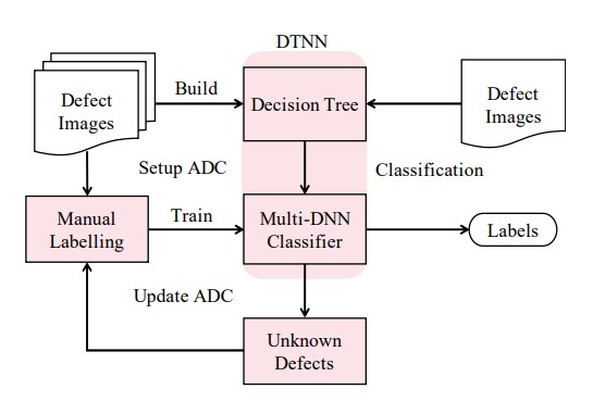
Automated defect classification (ADC) using images from optical microscopes or SEMs, or both, is the most widely used approach for defect analysis in fabs. Many state-of-the-art ADC methods are based on convolutional neural networks (CNNs). However, typical CNNs cannot achieve the high classification accuracy needed in semiconductors, and they are expensive.
Synopsys engineers recently found that a decision tree deep learning method can classify 98% of defects and features at 60X faster retraining time than traditional CNNs. The decision tree utilizes 8 CNNs and ResNet to automatically classify 12 defect types with images from SEM and optical tools (see figure 1). They presented their results at the SEMI’s recent Advanced Semiconductor Manufacturing Conference (ASMC).[1][…]

Read more: www.semiengineering.com


Where neural networks are being deployed in semiconductor manufacturing and how well they’re performing.
Copyright: semiengineering.com – “Improving Yield With Machine Learning”
Image source: Synopsys/IEEE ASMC
This is especially important in process control, where data sets are noisy. Neural networks can identify patterns that exceed human capability, or perform classification faster. Consequently, they are being deployed across a variety of manufacturing processes to spot defects and determine whether they will affect the functioning of a device over its anticipated lifetime.
“A lot of AI stuff is starting to happen now, where customers are identifying the most relevant measurements,” said Subodh Kulkarni, president and CEO of CyberOptics. “We extract the outliers, and the integration happens one level above, leading to new levels of yield improvement.”
Machine learning has been in use in the inspection arena for the longest of any manufacturing process, and it is being incorporated into new tools. Algorithms can isolate defect signatures or patterns that are unknown to the yield engineer.
“KLA’s broadband optical inspection systems have on-tool binning technology that uses defect attributes to separate detected events into different defect types and nuisance defects using machine learning,” said Satya Kurada, vice president of marketing at KLA.
Thank you for reading this post, don't forget to subscribe to our AI NAVIGATOR!
Defects identified on optical tools that require additional classification are typically reviewed on e-beam inspection systems. “Fab engineers use the defect information to optimize the production line,” Kurada said. “The end result should be more good die making it to end of line, where probe takes place.”
Like the human brain, deep learning (DL) recognizes patterns and uses that information to judge incoming data automatically. Using a cascade of multilayer, nonlinear processing units for feature extraction and transformation, each layer in a neural network uses the output of the previous layer as input for the next layer. In defect inspection, DL- or ML-based algorithms reduce the burden of manual classification and reduce time to result.
The automated nature of the networks also makes them attractive. “Because a deep learning model instantly updates itself, there’s less maintenance,” said Mike McIntyre, director of software product management at Onto Innovation. “But you also can’t do the diagnostic. That’s the thrill of this new modeling. I have less effort for maintenance than I would with my old machine logic models, where I would constantly have to tweak a slope, or an intercept, or a variable to make sure it remains consistent. So it’s important to trust but verify with different datasets. Also, these software solutions are not ‘set it and forget it.’ Our True ADC is a process tool, just like any other in the factory.”
Streamlining ADC
Automated defect classification (ADC) using images from optical microscopes or SEMs, or both, is the most widely used approach for defect analysis in fabs. Many state-of-the-art ADC methods are based on convolutional neural networks (CNNs). However, typical CNNs cannot achieve the high classification accuracy needed in semiconductors, and they are expensive.
Synopsys engineers recently found that a decision tree deep learning method can classify 98% of defects and features at 60X faster retraining time than traditional CNNs. The decision tree utilizes 8 CNNs and ResNet to automatically classify 12 defect types with images from SEM and optical tools (see figure 1). They presented their results at the SEMI’s recent Advanced Semiconductor Manufacturing Conference (ASMC).[1][…]
Read more: www.semiengineering.com
Share this: